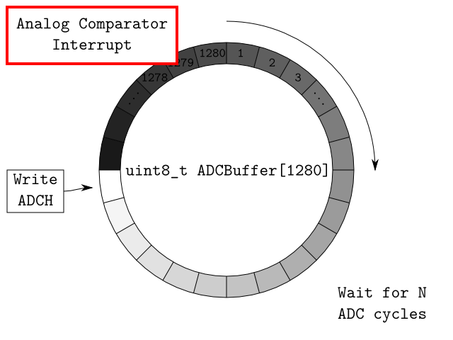
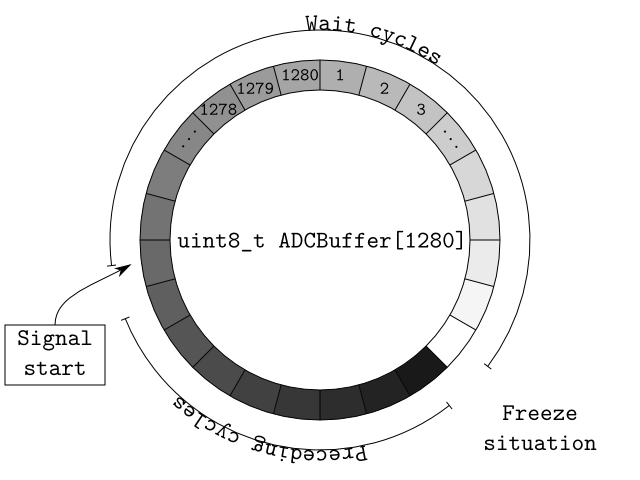
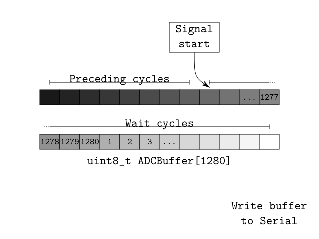
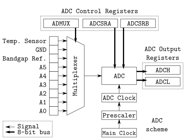
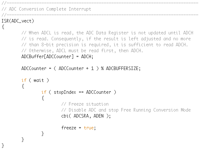
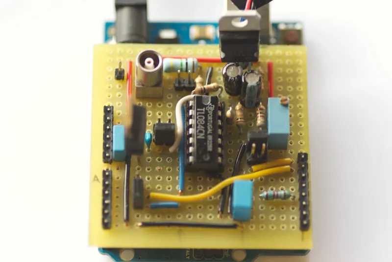
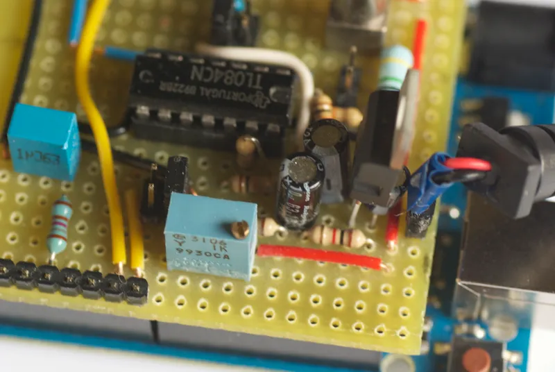
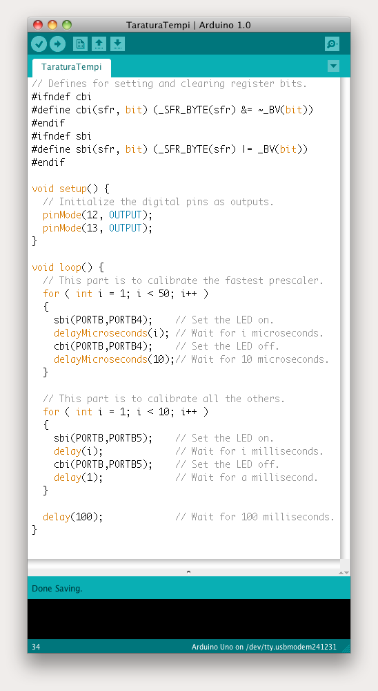
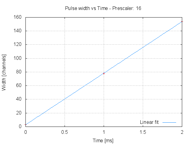
In the sketch, I wrote a initialization function that sets-up all the parameters of the ADC functioning. As I tend to write clean and commented code, I will just past the function here. We can refer to the preceding step and to the comments for the meaning of the registers.
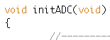
void initADC(void)
{
//---------------------------------------------------------------------
// ADMUX settings
//---------------------------------------------------------------------
// These bits select the voltage reference for the ADC. If these bits
// are changed during a conversion, the change will not go in effect
// until this conversion is complete (ADIF in ADCSRA is set). The
// internal voltage reference options may not be used if an external
// reference voltage is being applied to the AREF pin.
// REFS1 REFS0 Voltage reference
// 0 0 AREF, Internal Vref turned off
// 0 1 AVCC with external capacitor at AREF pin
// 1 0 Reserved
// 1 1 Internal 1.1V Voltage Reference with external
// capacitor at AREF pin
cbi(ADMUX,REFS1);
sbi(ADMUX,REFS0);
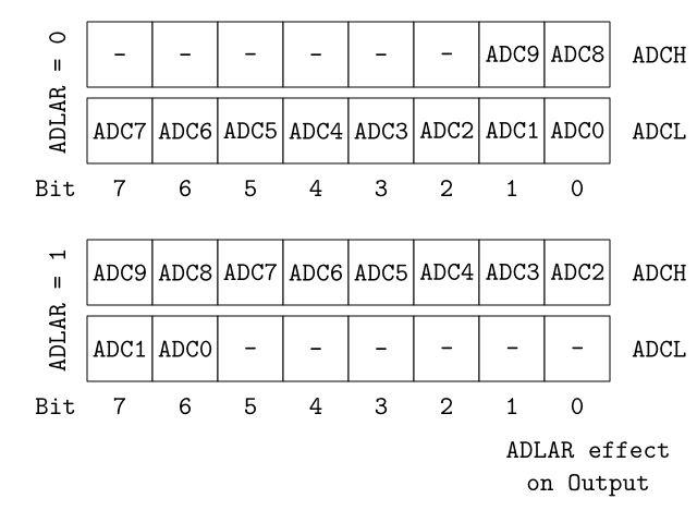
// The ADLAR bit affects the presentation of the ADC conversion result
// in the ADC Data Register. Write one to ADLAR to left adjust the
// result. Otherwise, the result is right adjusted. Changing the ADLAR
// bit will affect the ADC Data Register immediately, regardless of any
// ongoing conversions.
sbi(ADMUX,ADLAR);
// The value of these bits selects which analog inputs are connected to
// the ADC. If these bits are changed during a conversion, the change
// will not go in effect until this conversion is complete (ADIF in
// ADCSRA is set).
ADMUX |= ( ADCPIN & 0x07 );
//---------------------------------------------------------------------
// ADCSRA settings
//---------------------------------------------------------------------
// Writing this bit to one enables the ADC. By writing it to zero, the
// ADC is turned off. Turning the ADC off while a conversion is in
// progress, will terminate this conversion.
cbi(ADCSRA,ADEN);
// In Single Conversion mode, write this bit to one to start each
// conversion. In Free Running mode, write this bit to one to start the
// first conversion. The first conversion after ADSC has been written
// after the ADC has been enabled, or if ADSC is written at the same
// time as the ADC is enabled, will take 25 ADC clock cycles instead of
// the normal 13. This first conversion performs initialization of the
// ADC. ADSC will read as one as long as a conversion is in progress.
// When the conversion is complete, it returns to zero. Writing zero to
// this bit has no effect.
cbi(ADCSRA,ADSC);
// When this bit is written to one, Auto Triggering of the ADC is
// enabled. The ADC will start a conversion on a positive edge of the
// selected trigger signal. The trigger source is selected by setting
// the ADC Trigger Select bits, ADTS in ADCSRB.
sbi(ADCSRA,ADATE);
// When this bit is written to one and the I-bit in SREG is set, the
// ADC Conversion Complete Interrupt is activated.
sbi(ADCSRA,ADIE);
// These bits determine the division factor between the system clock
// frequency and the input clock to the ADC.
// ADPS2 ADPS1 ADPS0 Division Factor
// 0 0 0 2
// 0 0 1 2
// 0 1 0 4
// 0 1 1 8
// 1 0 0 16
// 1 0 1 32
// 1 1 0 64
// 1 1 1 128
sbi(ADCSRA,ADPS2);
sbi(ADCSRA,ADPS1);
sbi(ADCSRA,ADPS0);
//---------------------------------------------------------------------
// ADCSRB settings
//---------------------------------------------------------------------
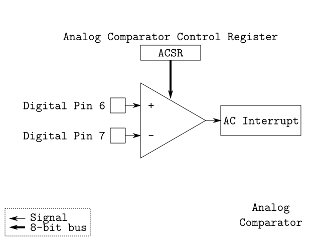
// When this bit is written logic one and the ADC is switched off
// (ADEN in ADCSRA is zero), the ADC multiplexer selects the negative
// input to the Analog Comparator. When this bit is written logic zero,
// AIN1 is applied to the negative input of the Analog Comparator.
cbi(ADCSRB,ACME);
// If ADATE in ADCSRA is written to one, the value of these bits
// selects which source will trigger an ADC conversion. If ADATE is
// cleared, the ADTS2:0 settings will have no effect. A conversion will
// be triggered by the rising edge of the selected Interrupt Flag. Note
// that switching from a trigger source that is cleared to a trigger
// source that is set, will generate a positive edge on the trigger
// signal. If ADEN in ADCSRA is set, this will start a conversion.
// Switching to Free Running mode (ADTS[2:0]=0) will not cause a
// trigger event, even if the ADC Interrupt Flag is set.
// ADTS2 ADTS1 ADTS0 Trigger source
// 0 0 0 Free Running mode
// 0 0 1 Analog Comparator
// 0 1 0 External Interrupt Request 0
// 0 1 1 Timer/Counter0 Compare Match A
// 1 0 0 Timer/Counter0 Overflow
// 1 0 1 Timer/Counter1 Compare Match B
// 1 1 0 Timer/Counter1 Overflow
// 1 1 1 Timer/Counter1 Capture Event
cbi(ADCSRB,ADTS2);
cbi(ADCSRB,ADTS1);
cbi(ADCSRB,ADTS0);
//---------------------------------------------------------------------
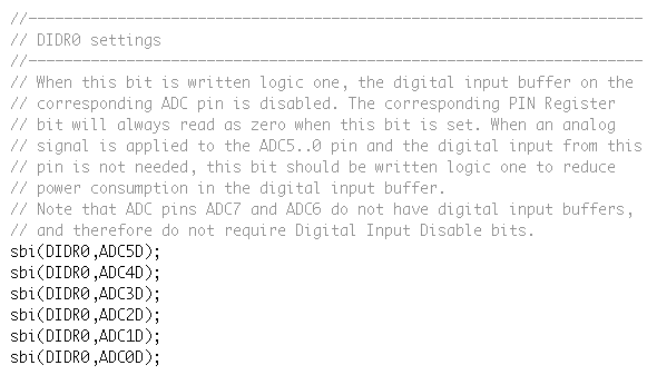
// DIDR0 settings
//---------------------------------------------------------------------
// When this bit is written logic one, the digital input buffer on the
// corresponding ADC pin is disabled. The corresponding PIN Register
// bit will always read as zero when this bit is set. When an analog
// signal is applied to the ADC5..0 pin and the digital input from this
// pin is not needed, this bit should be written logic one to reduce
// power consumption in the digital input buffer.
// Note that ADC pins ADC7 and ADC6 do not have digital input buffers,
// and therefore do not require Digital Input Disable bits.
sbi(DIDR0,ADC5D);
sbi(DIDR0,ADC4D);
sbi(DIDR0,ADC3D);
sbi(DIDR0,ADC2D);
sbi(DIDR0,ADC1D);
sbi(DIDR0,ADC0D);
}